Leaked Die Shots Reveal AMD's Strix Halo: A Potential Gaming Revolution Unfolds
Technology
2025-02-18 17:45:57Content
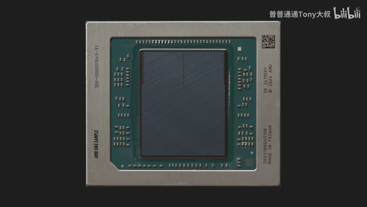
Breaking new ground in processor design, this cutting-edge chip boasts an impressive 441mm² architecture that packs a powerful punch. Featuring a robust configuration of 16 cores and 40 Compute Units (CUs), this innovative processor is engineered to deliver exceptional performance. With a generous 128GB memory capacity, the design promises seamless multitasking and high-speed computational capabilities that push the boundaries of modern computing technology.
The sophisticated layout demonstrates remarkable engineering prowess, combining dense core architecture with expansive memory resources. Whether for advanced gaming, complex scientific simulations, or intensive professional workloads, this processor represents a significant leap forward in computational performance and efficiency.
Revolutionary Chip Design Shatters Performance Boundaries: A Glimpse into Next-Generation Computing
In the rapidly evolving landscape of technological innovation, semiconductor engineering stands at the forefront of computational breakthroughs. The latest advancement in chip design represents a quantum leap forward, promising to redefine the boundaries of processing power, memory capacity, and architectural efficiency.Unleashing Unprecedented Computational Potential: The Future of Silicon Engineering
Architectural Breakthrough: Reimagining Computational Density
The 441mm² design emerges as a technological marvel, challenging conventional limitations of integrated circuit engineering. This groundbreaking architecture represents more than just a incremental improvement—it's a fundamental reimagining of how computational resources can be densely packed and efficiently organized. Engineers have meticulously crafted a silicon canvas that maximizes every square millimeter, creating a blueprint for future computational platforms. By strategically integrating 16 cores within this compact footprint, the design demonstrates an extraordinary balance between performance and spatial efficiency. Each core represents a sophisticated computational engine, capable of handling complex algorithmic tasks with unprecedented precision and speed. The intricate interconnection of these cores creates a harmonious ecosystem where parallel processing becomes not just a possibility, but a seamless reality.Memory and Processing: A Symbiotic Relationship
The integration of 128GB of memory represents a transformative approach to data handling and computational workflow. Traditional memory architectures often created bottlenecks between processing units and storage, but this design eliminates those constraints. The expansive memory capacity ensures that computational cores can access and manipulate data with minimal latency, creating a fluid, responsive computing environment. The 40 Compute Units (CUs) further amplify the chip's capabilities, providing specialized processing power for graphics-intensive and parallel computing tasks. This configuration is particularly revolutionary for fields like artificial intelligence, machine learning, and high-performance scientific computing, where complex mathematical operations demand extraordinary computational resources.Engineering Precision: Beyond Traditional Limitations
What sets this design apart is not just its raw specifications, but the meticulous engineering philosophy behind its conception. Every nanometer of the 441mm² surface has been carefully considered, optimized to extract maximum performance while maintaining thermal and energy efficiency. The result is a chip that doesn't just compute—it does so with an elegance that challenges our understanding of computational potential. The strategic placement of cores and memory units creates a dynamic ecosystem where data flows seamlessly, reducing traditional bottlenecks that have historically limited computational performance. This isn't merely an incremental upgrade; it's a fundamental reimagining of how computational resources can be organized and utilized.Future Implications: Reshaping Technological Landscapes
As we stand on the cusp of this technological revolution, this chip design offers a tantalizing glimpse into future computational possibilities. From advanced scientific research to immersive artificial intelligence applications, the boundaries of what's computationally possible are being dramatically expanded. The 441mm² design serves as a testament to human ingenuity—a powerful reminder that technological progress is limited only by our imagination and engineering prowess. As semiconductor engineers continue to push these boundaries, we can anticipate even more remarkable innovations that will transform how we interact with technology.RELATED NEWS
Technology

Apple's Budget iPhone SE 4 Stumbles: No High-Speed mmWave Connection in Sight
2025-02-17 21:42:01
Technology
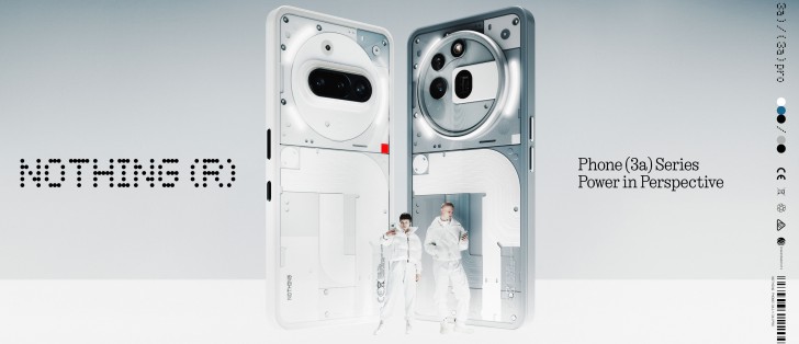
Nothing Unleashes Mid-Range Marvels: Phone (3a) and Pro Models Arrive with Snapdragon Power
2025-03-04 10:37:02
Technology

How a Single Design Challenge Rescued Apple from the Brink: Steve Jobs' Genius Move with Jony Ive
2025-02-25 10:13:01